


PCB Design & Fabrication (Prototype Development Process) - Industry Internship cum Training Program (Hybrid)
- Rajasekar Madhavan

- Jun 4
- 6 min read
Updated: Jun 18
Last date to Enroll: 19th June 2026 Registration Fee: INR 1200
ABOUT THE COURSE AREA:
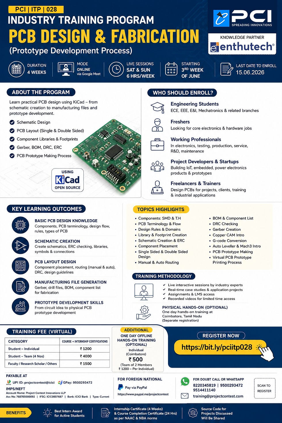
This one-month KiCad PCB Design course is designed for students, freshers, electronics engineers, project developers, and working professionals who want to learn practical PCB design from a basic level to an industrial level. KiCad is an open-source PCB design software used for schematic creation, PCB layout, component footprint generation, routing, 3D PCB viewing, BOM creation, ERC/DRC checking, Gerber generation, and PCB manufacturing file preparation. In this course, learners will study basic electronics components, SMD and through-hole components, PCB terminology, PCB design flow, design rules, component placement guidelines, single-sided and double-sided PCB design, manual routing, auto routing, library creation, footprint generation, Gerber creation, CopperCAM introduction, G-code conversion, AutoLeveller, Mach3 software, and PCB prototype making process. This course is highly useful for electronics product development, embedded system hardware design, power electronics, IoT product design, industrial automation, academic projects, PCB prototyping, and startup product development. After completing this course, students can apply for job roles such as PCB Design Engineer, PCB Layout Engineer, Hardware Design Engineer, Embedded Hardware Engineer, Power Electronics Design Engineer, R&D Engineer, Product Development Engineer, PCB CAM Engineer, Electronics Manufacturing Engineer, and Freelance PCB Designer. PCB design skills are useful in many companies, such as Tessolve Semiconductor, Centum Electronics, VVDN Technologies, Syrma SGS Technology, Avalon Technologies, Kaynes Technology, Sanmina, Foxconn, Dixon Technologies, Zetwerk, Smile Electronics, RioSH Technologies, MicroLOGIX, Zettaone Technologies, Sunstream Global Technologies, and other electronics design, embedded systems, PCB manufacturing, EMS, automotive electronics, telecom, defence electronics, industrial automation, and power electronics companies. Overall, this course helps learners convert electronic circuit ideas into professional PCB designs and prepares them for real-time electronics design and manufacturing industries.
LEARNING OUTCOME:
By the end of this course, participants will be able to:
1. Basic PCB Design Knowledge: Learners will understand basic electronic components, PCB terminology, SMD components, through-hole components, and PCB design flow. This helps them start PCB design from the foundation level with proper technical understanding.
2. Schematic Creation in KiCad: Learners will create circuit schematics using symbols, libraries, wires, labels, and proper electrical connections. They will also learn ERC checking to identify and correct schematic-level errors.
3. PCB Layout Design: Learners will design single-sided and double-sided PCB layouts using proper component placement and routing techniques. They will understand design rules, track width, clearance, layer usage, and layout best practices.
4. Manufacturing File Generation: Learners will generate Gerber files, drill files, BOM, and component lists required for PCB fabrication. This helps them convert a completed PCB design into production-ready manufacturing output.
5. Prototype Development Skills: Learners will understand the complete PCB prototype-making process from circuit idea to physical board development.
TRAINING CUM INTERNSHIP PLAN:
Internship Duration: 4 Weeks
Live session: Sat & Sun – 6 hrs/week
Last Date to Enrol: 19/6/2026
Starting Date: 20th June
Internship Mode: Online via Google Meet
Additional: One Day Physical Hands-on (Optional)
Recorded Videos will be provided for a limited time access
EVENT ID: PCIITP028
Join Our WhatsApp Group for instant updates on Training & Contest:

ABOUT THE INTERNSHIP CUM TRAINING PROGRAM (ONLINE):
Project Contest Innovations (PCI) LLP., in association with various Industries across India, has partnered to provide various trainings on the emerging areas to students, faculty, research scholars & start-ups with industry-relevant expertise, to enhance their employability and entrepreneurial capabilities. The Program delivers a task-driven training model that provides participants with hands-on experience. The program is structured to simulate an internship environment, ensuring practical exposure to live projects handled by industry experts.
Key Features
Industry Certification: Participants receive a recognised certification upon successful completion.
Expert-Led Sessions: Training is conducted by professionals actively working on real-world projects.
Hybrid Learning Model: The program offers both online and offline engagement.
Wide Reach: Over 5,000+ students from 250+ institutions have benefited from PCI’s training initiatives.
Comprehensive Course Areas: Topics include Artificial Intelligence & IoT, Electrical Vehicle Design & Fabrication, and other emerging technologies.
Benefits
Skill Enhancement: Gain expertise in cutting-edge technologies.
Internship Exposure: Experience industry workflows and project execution.
Networking Opportunities: Connect with professionals and peers in the field.
Career Advancement: Improve employability and entrepreneurial prospects.
PCI’s Training Program is a gateway for aspiring innovators to bridge the gap between academic learning and industry requirements. Whether you are a student looking to gain practical knowledge or a startup aiming to refine your technical skills, this program offers a structured pathway to success.
SAMPLE CERTIFICATE:

Registration Link:
SYLLABUS TO BE COVERED DURING LIVE SESSIONS:
Types of Electronic Components
SMD and T.H Mounting Technology
Passive Components SMD Package Type
Active Components SMD Package Type
PCB Terminology
PCB Design Flow
Design Rules
PCB Domain
Electronics Circuits
Types of PCB
Substrate Types
PCB Connection
EDA Tools Software
PCB Standards
Component Placement guidelines
PCB Prototype Making Process
PCB Prototype Designing Tools
PCB Designing Layout
Classes for PCB Design
Important for Design Elements
PCB Designing guidelines
Hands on Training in Kicad Software
Library Creation & Footprint generation for SMD and T.H components
Uses of Grids
Library searching
Schematic Creations
Single Sided Design
Component Placement
Component Arrangement
Double Sided Design
Connection Process
BOM Creation
ERC Checking
Layout Creations
Auto Routing
Manual routing
Component list Creation
DRC Checking
Gerber Creation
Copper CAM Introduction
Covert from Gerber to G code
Auto leveller software Introduction
Mach3 Software Introduction
PCB Prototype Making process
Virtual PCB Prototype Printing Process
Hardware & Software to be Used:
Software to be Used:
1. Open Source Kicad Software
TRAINING REQUIREMENTS:
1. A desktop or laptop computer is required. Windows 7 is recommended.
2. Stable internet connection
3. A microphone is strongly recommended for trainer-student communication.
GUIDELINES:
Only limited registration is allowed based on first cum first confirmation process.
Internship cum Training Certificate (4 Weeks) Certificate for students will be jointly issued by Training Industry & Project Contest Innovations LLP
If students enrol as 4 Members, the faculty mentor of the team will get a separate Faculty Mentor Certificate
Payment to be done in the Project Contest Innovations LLP Account & a screenshot to be uploaded in the registration link
Important: Transfer of participation to another student is not allowed
Note: Recorded Video will be given for limited access time if Live Session is missed
BENEFITS:
Active students will be given the Best Intern Award, decided by the Industrial trainer.
Internship cum Training Certificate (4 Weeks) will be issued as per the norms specified in AICTE Internship Policy, NAAC & NBA Accreditation process
WHO CAN ENROLL:
1. Engineering Students
Students from ECE, EEE, E&I, Mechatronics, and related branches can join this course to learn practical PCB design skills for academic projects and future jobs.
2. Freshers Looking for Core Electronics Jobs
Freshers who want to enter PCB design, hardware design, embedded systems, power electronics, and electronics manufacturing fields can benefit from this course.
3. Working Professionals in Electronics
Engineers already working in electronics, testing, production, service, or maintenance can join to upgrade their PCB design and product development skills.
4. Project Developers and Startup Teams
Anyone developing electronic products, IoT devices, sensor boards, power supply boards, or embedded system prototypes can enrol to convert circuit ideas into real PCB designs.
5. Freelancers and Trainers
Freelancers, technical trainers, and project centre teams can join this course to design PCBs for students, clients, startups, and industrial applications.
Registration Link: https://bit.ly/pciitp028
TRAINING METHODOLOGY:
Online Mode:
1. Real-Time Case Studies & Application Project.
2. Interact with an industry training expert and work on real-life challenges
3. Complete Plan of the Live sessions and Class Link will be shared with registered participants through the Program WhatsApp Group
4. Assignments after each topic of the training will be provided to the students for practice
5. All training materials developed remain the intellectual property of the training Industry. it has to be used only under their approval and/or supervision.
Physical Visit: (For Special Enrolled Candidates)
Based on special registration, a one-day physical hands-on will be provided at Enthu Tech Branch Office at Coimbatore, Tamil Nadu. Travel arrangements have to be taken care of by participants.
TRAINING FEE:
Online Mode Only:
Individual Registration: 1,200 INR
Four-member team: 4,000 INR
Others: (Research Scholar, Faculty & Job Seekers)
Individual Registration: 1,500 INR
One day Offline Hands-on Training (Optional):
Per Member: 500 INR
PAYMENT MODE: UPI ID: projectcontest@icici
GPAY: 9500293472
IMPS/NEFT:
Account Name: Project Contest Innovations LLP
Acc no: 768705000092
IFSC: ICIC0007687
Bank: ICICI Bank
Type: Current
LIST OF E-CERTIFICATES:
Confirmation Letter
Internship cum Training Certificate Certificate
Best Intern Award Certificate for TOP Performers
Faculty Mentor Certificate for Teams
For Doubt call or WhatsApp: 8220345819, 9500293472, 9514411140
eMail: training@projectcontest.com
............Lets Learn Together............
For registration click the form link below(Upload payment screenshot):
Register Now: https://bit.ly/pciitp028
Category: Industry Internship, Training, MetaVerse
For Instant Alerts:
Projectcontest LinkedIn Page: www.linkedin.com/company/project-contest
ProjectContest YouTube: www.youtube.com/c/projectcontest
ProjectContest Instagram: www.instagram.com/projectcontest
Follow Rajasekar Madhavan: www.linkedin.com/in/rajasekarmadhavan
Disclaimer: The Internship/Training is organised through the Industry Training Partnership (ITP) program of Project Contest Innovations (PCI) LLP, with the partnered Industry, to share the knowledge of the resource person/Industry with the Innovators, Students, and the public. Certificates will be issued to participants only upon meeting all the required parameters at the time of Program launch. PCI and the Industry Partner have the right to cancel the Internship due to an unavoidable situation without prior information, if money is paid, alternate days will be informed on such circumstances or the money will be returned. Participants, once registered, are not allowed to cancel or transfer the registration, and money will not be reimbursed. Let's Learn Together!!!


Comments